
 Space.com
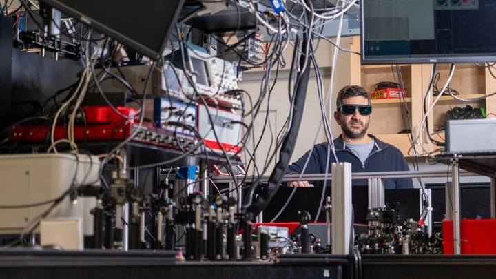
Crystals used in applications as varied as lasers, LEDs and the semiconductors used in sensors found in astronomical instruments could someday be 'drawn' rather than 'grown', leading to higher performance and lower costs.
A team led by Elad Harel of Michigan State University has used a laser to heat a gold nanoparticle, which then triggers crystal formation within a solution of lead halide perovskite. By moving the gold nanoparticle, again using lasers, it is therefore possible, in theory, to precisely 'draw' the crystals exactly where they need to be in an electronic device.
Crystals used in electronics are traditionally made through a variety of techniques, such as vapor diffusion, whereby the crystal precipitates out of a solution, or through planting a crystal 'seed' and then watchin

 WKOW 27
 TechCrunch
 FOX19 NOW
 WMBD-Radio
 KWWL
KWWL Detroit Free Press
 CBS Colorado
 Tech Times
 Bitcoinist
 PC World
 AlterNet